
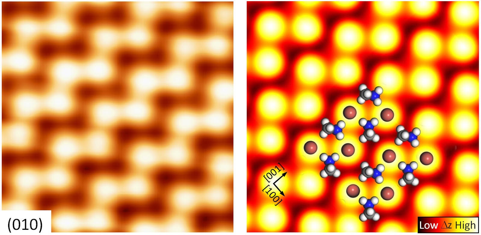
Topography image
of atoms of the perovskite crystal and calculated images
with position of
atoms and molecules indicated.
(January 8, 2016) Organic-inorganic
perovskite materials are key components of the new generation of solar cells.
Understanding properties of these materials is important for improving lifetime
and quality of solar cells. Researchers from the Energy Materials and Surface
Sciences (EMSS) Unit, led by Prof. Yabing Qi, at the Okinawa Institute of
Science and Technology Graduate University (OIST) in collaboration with Prof.
Youyong Li’s group from Soochow University (China) and Prof. Nam-Gyu Park’s
group from Sungkyunkwan University (Korea) report in the Journal of the
American Chemical Society the first atomic resolution study of
organic-inorganic perovskite.
Perovskites are a class of materials with the general
chemical formula ABX3. A and B are positive ions bound by negative ions X.
Organic-inorganic perovskites used in solar cells are usually methylammonium
lead halides (CH3NH3PbX3, where X is bromine, iodine, or chlorine). The OIST
scientists used a single crystal of methylammonium lead bromide (CH3NH3PbBr3)
to create topographic images of its surface with a scanning tunneling
microscope.

The researchers
discovered that methylammonium molecules (represented by a ball-and-stick model
in the centre) can
rotate and that they favour specific orientations that lead to two types of
surface
structures with
distinctly different properties (left and right images).
This microscope uses a conducting tip that moves across the
surface in a manner very similar to a finger moving across a Braille sign.
While the bumps in Braille signs are a few millimetres apart, the microscope
detects bumps that are more than million times smaller — atoms and molecules.
This is achieved by the quantum tunneling effect — the ability of an electron
to pass through a barrier. The probability of an electron passing between the
material surface and the tip depends on the distance between the two. The
resulting atomic-resolution topographic images reveal positions and
orientations of atoms and molecules, and also provide a detailed look at
structural defects in the surface.

Dr Robin Ohmann, first author of the paper, transfers a sample into the
scanning tunneling microscope.
"At room temperature atoms and molecules are quite
mobile, so we decided to freeze the crystal to almost absolute zero (-269ºC) to
get a good picture of its atomic structure,” says Dr Robin Ohmann, a member of
the EMSS Unit and the first author of the paper. The crystal was cut and
studied in a vacuum to avoid contamination of the surface. Dr Ohmann's
colleagues from Soochow University calculated atomic structures using
principles of quantum physics and then compared them with scanning tunneling
microscopy data.