January 31, 2016

Czech scientists solved the enigma of coexistence of people with Rh+ and Rh- blood groups


(January 31, 2016)  Before the advent of modern medicine, about 10 000 Rh positive children born to Rh negative mothers were dying for hemolytic anemia in the US each year. Without the superiority of the heterozygotes – the carriers of both variants of Rhesus gene, the less abundant allele should be quickly eliminated from any population. Jaroslav Flegr probably solved 80 years old enigma of coexistence of carriers of two variants of Rhesus gene in the same population.

A new study published today in PLoS ONE (1) showed that incidence and morbidity of many diseases and disorders correlate negatively with frequencies of Rh+ heterozygotes (i.e. the carriers of one copy of the gene for Rh positivity and one copy of the gene for Rh negativity) in the population of individual countries. At the same time, the disease burden associated with the same disorders correlated positively with frequency of Rh negative subjects in individual countries. Together with the observed worse health status and higher incidence of many disorders in Rh negative subjects published by the same research team last autumn (2), this result probably solved 80 years old enigma of coexistence of carriers of two variants of Rhesus gene in the same population.


journal reference (Open Access) >>

January 30, 2016

First self-assembled superconductor structure created


Lindsay France/University Photography
Group leader Ulrich Wiesner, right, the Spencer T. Olin Professor of Engineering,
and graduate student and co-lead author Peter Beaucage, second from right, hold models
of the self-assembled gyroid superconductor the group created. Also pictured are
Bruce van Dover, left, professor in the Department of Materials Science and Engineering,
and Sol Gruner, the John L. Wetherill Professor of Physics.

(January 30, 2016)  Building on nearly two decades’ worth of research, a multidisciplinary team at Cornell has blazed a new trail by creating a self-assembled, three-dimensional gyroidal superconductor.

Ulrich Wiesner, the Spencer T. Olin Professor of Engineering, led the group, which included researchers in engineering, chemistry and physics.

The group’s findings are detailed in a paper published in Science Advances, Jan. 29.

Wiesner said it’s the first time a superconductor, in this case niobium nitride (NbN), has self-assembled into a porous, 3-D gyroidal structure. The gyroid is a complex cubic structure based on a surface that divides space into two separate volumes that are interpenetrating and contain various spirals. Pores and the superconducting material have structural dimensions of only around 10 nanometers, which could lead to entirely novel property profiles of superconductors.

Superconductivity for practical uses, such as in magnetic resonance imaging (MRI) scanners and fusion reactors, is only possible at near absolute zero (-459.67 degrees below zero), although recent experimentation has yielded superconducting at a comparatively balmy 94 degrees below zero.

“There’s this effort in research to get superconducting at higher temperatures, so that you don’t have to cool anymore,” Wiesner said. “That would revolutionize everything. There’s a huge impetus to get that.”

Superconductivity, in which electrons flow without resistance and the resultant energy-sapping heat, is still an expensive proposition. MRIs use superconducting magnets, but the magnets constantly have to be cooled, usually with a combination of liquid helium and nitrogen.


journal reference (pdf) >>

Graphene shown to safely interact with neurons in the brain


(January 30, 2016)  Researchers have shown that graphene can be used to make electrodes that can be implanted in the brain, which could potentially be used to restore sensory functions for amputee or paralysed patients, or for individuals with motor disorders such as Parkinson’s disease. 

Researchers have successfully demonstrated how it is possible to interface graphene – a two-dimensional form of carbon – with neurons, or nerve cells, while maintaining the integrity of these vital cells. The work may be used to build graphene-based electrodes that can safely be implanted in the brain, offering promise for the restoration of sensory functions for amputee or paralysed patients, or for individuals with motor disorders such as epilepsy or Parkinson’s disease.

The research, published in the journal ACS Nano, was an interdisciplinary collaboration coordinated by the University of Trieste in Italy and the Cambridge Graphene Centre.

Previously, other groups had shown that it is possible to use treated graphene to interact with neurons. However the signal to noise ratio from this interface was very low. By developing methods of working with untreated graphene, the researchers retained the material’s electrical conductivity, making it a significantly bet


journal reference >>

Practice makes perfect, York U brain study confirms


(January 30, 2016)  In this study, Faculty of Health researchers were looking at fMRI brain scans of professional ballet dancers to measure the long-term effects of learning.

“We wanted to study how the brain gets activated with long-term rehearsal of complex dance motor sequences,” says Professor Joseph DeSouza, who studies and supports people with Parkinson’s disease. “The study outcome will help with understanding motor learning and developing effective treatments to rehabilitate the damaged or diseased brain.”

For the study, 11 dancers (19-50 years of age) from the National Ballet of Canada were asked to visualize dance movements to music, while undergoing fMRI scanning. The scans measured Blood-Oxygen-Level-Dependent (BOLD) contrasts at four time points over 34 weeks, when they were learning a new dance.

“Our aim was to find out the long-term impact of the cortical changes that occur as one goes from learning a motor sequence to becoming an expert at it,” says coauthor Rachel Bar, who was a ballet dancer herself. “Our results also suggest that understanding the neural underpinnings of complex motor tasks such as learning a new dance can be an effective model to study motor learning in the real world.”


journal reference (Open Access) >>

Nanosheet growth technique could revolutionize nanomaterial production


The new nanoscale manufacturing process draws zinc to the surface of a liquid,
where it forms sheets just a few atoms thick. XUDONG WANG

(January 30, 2016)  After six years of painstaking effort, a group of University of Wisconsin—Madison materials scientists believes the tiny sheets of the semiconductor zinc oxide they’re growing could have huge implications for the future of a host of electronic and biomedical devices.

The group — led by Xudong Wang, a UW–Madison professor of materials science and engineering, and postdoctoral researcher Fei Wang — has developed a technique for creating nearly two-dimensional sheets of compounds that do not naturally form such thin materials. It is the first time such a technique has been successful.

The researchers described their findings in the journal Nature Communications on Jan. 20.

Essentially the microscopic equivalent of a single sheet of paper, a 2-D nanosheet is a material just a few atoms thick. Nanomaterials have unique electronic and chemical properties compared to identically composed materials at larger, conventional scales.

read entire press  release >>

journal reference (Open Access) >>

NASA Engineers Tapped to Build First Integrated-Photonics Modem


A new-fangled modem that will employ an emerging technology called integrated
photonics will be tested as part of NASA’s Laser Communications Relay Demonstration mission.
Credits: NASA

(January 30, 2016)  A NASA team has been tapped to build a new type of communications modem that will employ an emerging, potentially revolutionary technology that could transform everything from telecommunications, medical imaging, advanced manufacturing to national defense.

The space agency’s first-ever integrated-photonics modem will be tested aboard the International Space Station beginning in 2020 as part of NASA’s multi-year Laser Communications Relay Demonstration, or LCRD. The cell phone-sized device incorporates optics-based functions, such as lasers, switches, and wires, onto a microchip — much like an integrated circuit found in all electronics hardware.

Once aboard the space station, the so-called Integrated LCRD LEO (Low-Earth Orbit) User Modem and Amplifier (ILLUMA) will serve as a low-Earth orbit terminal for NASA’s LCRD, demonstrating yet another capability for high-speed, laser-based communications.
Data Rates Demand New Technology

Since its inception in 1958, NASA has relied exclusively on radio frequency (RF)-based communications. Today, with missions demanding higher data rates than ever before, the need for LCRD has become more critical, said Don Cornwell, director of NASA’s Advanced Communication and Navigation Division within the space Communications and Navigation Program, which is funding the modem’s development.

LCRD promises to transform the way NASA sends and receives data, video and other information. It will use lasers to encode and transmit data at rates 10 to 100 times faster than today’s communications equipment, requiring significantly less mass and power. Such a leap in technology could deliver video and high-resolution measurements from spacecraft over planets across the solar system — permitting researchers to make detailed studies of conditions on other worlds, much as scientists today track hurricanes and other climate and environmental changes here on Earth.

read entire press  release >>

New Type of Nanowires, Built with Natural Gas Heating


(January 30, 2016)  UNIST research team, developed a new simple nanowire manufacturing technique.

A team of Korean researchers, affiliated with UNIST has recently pioneered in developing a new simple nanowire manufacturing technique that uses self-catalytic growth process assisted by thermal decomposition of natural gas. According to the research team, this method is simple, reproducible, size-controllable, and cost-effective in that lithium-ion batteries could also benefit from it.

In their approach, they discovered that germanium nanowires are grown by the reduction of germanium oxide particles and subsequent self-catalytic growth during the thermal decomposition of natural gas, and simultaneously, carbon sheath layers are uniformly coated on the nanowire surface.

This study is a collaboration among scientists, including Prof. SooJin Park (School of Energy and Chemical Engineering) and Prof. Sang Kyu Kwak (School of Energy and Chemical Engineering), Dr. Sinho Choi (UNIST), Combined M.S./Ph.D. Student Dae Yeon Hwang (UNIST), and Researcher Jieun Kim (Korea Research Institute of Chemical Technology).


In a study, reported in the January 21, 2016 issue of Nano Letters, the team demonstrated a new redox-responsive assembly method to synthesize hierarchically structured carbon-sheathed germanium nanowires (c-GeNWs) on a large scale by the use of self-catalytic growth process assisted by thermally decomposed natural gas.

According to the team, this simple synthetic process not only enables them to synthesize hierachially assembled materials from inexpensive metal oxides at a larger scale, but also can likely be extended to other metal oxides as well. Moreover, the resulting hierarchically assembled nanowires (C-GeNWs) show enhanced chemical and thermal stability, as well as outstanding electrochemical properties.


journal reference >>

January 28, 2016

Scientists decode brain signals nearly at speed of perception


Subjects viewed a random sequence of images of faces and houses and were asked
to look for an inverted house like the one at bottom left. "That was a distractor,"
Jeff Ojemann said. "We were interested in what the brain was doing at the other times."
Illustration by Kai Miller and Brian Donohue

(January 28, 2016) Electrodes in patients’ temporal lobes carry information that, when analyzed, enables scientists to predict what object patients are seeing

Using electrodes implanted in the temporal lobes of awake patients, scientists have decoded brain signals at nearly the speed of perception.  Further, analysis of patients’ neural responses to two categories of visual stimuli – images of faces and houses – enabled the scientists to subsequently predict which images the patients were viewing, and when, with better than 95 percent accuracy.

The research is published today in PLOS Computational Biology.

University of Washington computational neuroscientist Rajesh Rao and UW Medicine neurosurgeon Jeff Ojemann, working their student Kai Miller and with colleagues in Southern California and New York, conducted the study.

“We were trying to understand, first, how the human brain perceives objects in the temporal lobe, and second, how one could use a computer to extract and predict what someone is seeing in real time?” explained Rao.  He is a UW professor of computer science and engineering, and he directs the National Science Foundation’s Center for Sensorimotor Engineering, headquartered at UW. 


The numbers 1-4 denote electrode placement in temporal lobe,
and neural responses of two signal types being measured.

“Clinically, you could think of our result as a proof of concept toward building a communication mechanism for patients who are paralyzed or have had a stroke and are completely locked-in,” he said.

The study involved seven epilepsy patients receiving care at Harborview Medical Center in Seattle. Each was experiencing epileptic seizures not relieved by medication, Ojemann said, so each had undergone surgery in which their brains’ temporal lobes were implanted – temporarily, for about a week – with electrodes to try to locate the seizures’ focal points.

Neuroscientist Rajesh Rao and neurosurgeon Jeff Ojemann
are faculty at the University of Washington.

“They were going to get the electrodes no matter what; we were just giving them additional tasks to do during their hospital stay while they are otherwise just waiting around,” Ojemann said.

Temporal lobes process sensory input and are a common site of epileptic seizures. Situated behind mammals’ eyes and ears, the lobes are also involved in Alzheimer’s and dementias and appear somewhat more vulnerable than other brain structures to head traumas, he said.


In the experiment, the electrodes from multiple temporal-lobe locations were connected to powerful computational software that extracted two characteristic properties of the brain signal: “event-related potentials” and “broadband spectral changes.”


read also (UW. Neural Systems Laboratory) >>

Identifying another piece in the Parkinson's disease pathology puzzle


Parkinson’s researchers used proteomics to identify Rab proteins as a physiological
substrate of LRRK2, a Parkinson’s drug target. This finding may accelerate current
research and open a novel therapeutic avenue. © MPI f. Biochemistry

(January 28, 2016)  International consortium identifies and validates cellular role of priority Parkinson’s disease drug target, LRRK2 kinase

An international public-private consortium of researchers led by The Michael J. Fox Foundation for Parkinson’s Research has had its work published in eLife. A team comprising investigators from the Max Planck Institute of Biochemistry, the University of Dundee, GlaxoSmithKline and MSD, known as Merck & Co., Inc., in the United States and Canada, has discovered that the LRRK2 kinase regulates cellular trafficking by deactivating Rab proteins. This finding illuminates a novel route for therapeutic development and may accelerate testing of LRRK2 inhibitors as a disease-modifying therapy for Parkinson’s, the second most common neurodegenerative disease.

An international public-private research consortium has identified and validated a cellular role of a primary Parkinson’s disease drug target, the LRRK2 kinase. This important finding, published in the online, open-access eLife journal, illuminates a novel route for therapeutic development and intervention testing for Parkinson’s, the second most common neurodegenerative disease after Alzheimer’s.

A team of investigators from the Max Planck Institute of Biochemistry, the University of Dundee, The Michael J. Fox Foundation for Parkinson’s Research (MJFF), GlaxoSmithKline (GSK) and MSD contributed unique tools and expertise toward rigorous systematic testing that determined the LRRK2 kinase regulates cellular trafficking by deactivating certain Rab proteins (3, 8, 10 and 12).

read entire press  release >>

RESEARCHERS DEVELOP COMPLETELY NEW KIND OF POLYMER


Northwestern University researchers have developed a new hybrid polymer with
removable supramolecular compartments, shown in this molecular model.
(Credit: Mark E. Seniw, Northwestern University)

(January 28, 2016)  Hybrid polymers could lead to new concepts in self-repairing materials, drug delivery and artificial muscles

Imagine a polymer with removable parts that can deliver something to the environment and then be chemically regenerated to function again. Or a polymer that can lift weights, contracting and expanding the way muscles do.

These functions require polymers with both rigid and soft nano-sized compartments with extremely different properties that are organized in specific ways. A completely new hybrid polymer of this type has been developed by Northwestern University researchers that might one day be used in artificial muscles or other life-like materials; for delivery of drugs, biomolecules or other chemicals; in materials with self-repair capability; and for replaceable energy sources.

“We have created a surprising new polymer with nano-sized compartments that can be removed and chemically regenerated multiple times,” said materials scientist Samuel I. Stupp, the senior author of the study.

“Some of the nanoscale compartments contain rigid conventional polymers, but others contain the so-called supramolecular polymers, which can respond rapidly to stimuli, be delivered to the environment and then be easily regenerated again in the same locations. The supramolecular soft compartments could be animated to generate polymers with the functions we see in living things,” he said.

Stupp is director of Northwestern’s Simpson Querrey Institute for BioNanotechnology. He is a leader in the fields of nanoscience and supramolecular self-assembly, the strategy used by biology to create highly functional ordered structures.

read entire press  release >>

Putting Silicon ‘Sawdust’ in a Graphene Cage Boosts Battery Performance


To build graphene cages around silicon particles, researchers coated the particles with nickel;
grew layers of graphene on top of the nickel; and used acid to dissolve the nickel away, leaving
enough space for the silicon to expand inside the cage. (Y. Li et al., Nature Energy)

(January 28, 2016)  Approach Could Remove Major Obstacles to Increasing the Capacity of Lithium-ion Batteries

Scientists have been trying for years to make a practical lithium-ion battery anode out of silicon, which could store 10 times more energy per charge than today’s commercial anodes and make high-performance batteries a lot smaller and lighter. But two major problems have stood in the way: Silicon particles swell, crack and shatter during battery charging, and they react with the battery electrolyte to form a coating that saps their performance.

Now, a team from Stanford University and the Department of Energy’s SLAC National Accelerator Laboratory has come up with a possible solution: Wrap each and every silicon anode particle in a custom-fit cage made of graphene, a pure form of carbon that is the thinnest and strongest material known and a great conductor of electricity.

In a report published Jan. 25 in Nature Energy, they describe a simple, three-step method for building microscopic graphene cages of just the right size: roomy enough to let the silicon particle expand as the battery charges, yet tight enough to hold all the pieces together when the particle falls apart, so it can continue to function at high capacity. The strong, flexible cages also block destructive chemical reactions with the electrolyte.

 This time-lapse movie from an electron microscope shows the new battery material in action:
a silicon particle expanding and cracking inside a graphene cage while being charged.
The cage holds the pieces of the particle together and preserves its electrical conductivity
and performance. (Hyun-Wook Lee/Stanford University)

“In testing, the graphene cages actually enhanced the electrical conductivity of the particles and provided high charge capacity, chemical stability and efficiency," said Yi Cui, an associate professor at SLAC and Stanford who led the research. “The method can be applied to other electrode materials, too, making energy-dense, low-cost battery materials a realistic possibility.”

The Quest for Silicon Anodes

Lithium-ion batteries work by moving lithium ions back and forth through an electrolyte solution between two electrodes, the cathode and the anode. Charging the battery forces the ions into the anode; using the battery to do work moves the ions back to the cathode.


journal reference >>

January 27, 2016

To Help Diabetics, Intelligent Socks Are Paired With Smartphones


Students at the Hebrew University's BioDesign program paired pressure-sensing
socks with smartphones to reduce foot ulcers in diabetic patients.
(Photo: The Hebrew University of Jerusalem)

(January 27, 2016)  Diabetic neuropathy is a type of nerve damage associated with the development of foot ulcers in patients with diabetes. Resulting from anatomical deformation, excessive pressure and poor blood supply, it affects over 130 million individuals worldwide. It is also the leading cause of amputation, costing the United States economy alone more than $10 billion annually.

Diabetic patients are encouraged to get regular checkups to monitor for the increased pressure and ulceration that can eventually require amputation. However, ulcers are only diagnosed after they occur, meaning that patients require healing time, which dramatically increases healthcare costs.

Members of the BioDesign: Medical Innovation program, created by The Hebrew University of Jerusalem and its affiliated Hadassah Medical Center, set out to solve this problem.

“This is a significant medical problem that affects the lives of millions. We thought there must be a way to avoid these wounds altogether,” said Danny Bavli, the group’s lead engineer. 


video >>

Let them see you sweat: What new wearable sensors can reveal from perspiration


UC Berkeley engineers put their wearable sweat sensors to the test. (UC Berkeley video
produced by Roxanne Makasdjian and Stephen McNally, UC Berkeley)

(January 27, 2016)  When UC Berkeley engineers say they are going to make you sweat, it is all in the name of science.

Specifically, it is for a flexible sensor system that can measure metabolites and electrolytes in sweat, calibrate the data based upon skin temperature and sync the results in real time to a smartphone.

While health monitors have exploded onto the consumer electronics scene over the past decade, researchers say this device, reported in the Jan. 28 issue of the journal Nature, is the first fully integrated electronic system that can provide continuous, non-invasive monitoring of multiple biochemicals in sweat.

The advance opens doors to wearable devices that alert users to health problems such as fatigue, dehydration and dangerously high body temperatures.

Users wearing the flexible sensor array can run and move freely while the chemicals in their
sweat are measured and analyzed. The resulting data, which is transmitted wirelessly
to a mobile device, can be used to help assess and monitor a user’s state of health.
(Image by Der-Hsien Lien and Hiroki Ota, UC Berkeley)

“Human sweat contains physiologically rich information, thus making it an attractive body fluid for non-invasive wearable sensors,” said study principal investigator Ali Javey, a UC Berkeley professor of electrical engineering and computer sciences. “However, sweat is complex and it is necessary to measure multiple targets to extract meaningful information about your state of health. In this regard, we have developed a fully integrated system that simultaneously and selectively measures multiple sweat analytes, and wirelessly transmits the processed data to a smartphone. Our work presents a technology platform for sweat-based health monitors.”


The new sensor developed at UC Berkeley can be made into “smart” wristbands
or headbands that provide continuous, real-time analysis of the chemicals in sweat.
(UC Berkeley photo by Wei Gao)

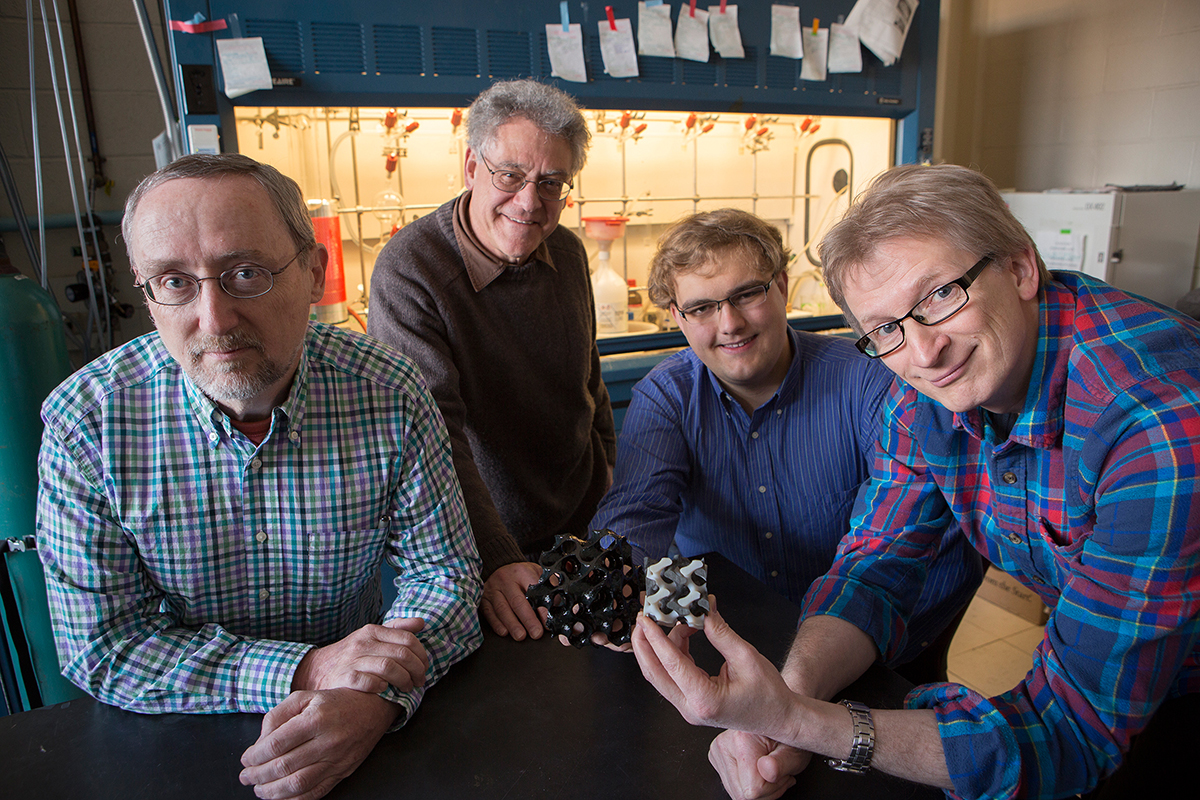
Javey worked with study co-lead authors Wei Gao and Sam Emaminejad, both of whom are postdoctoral fellows in his lab. Emaminejad also has a joint appointment at the Stanford School of Medicine, and all three have affiliations with the Berkeley Sensor and Actuator Center and the Materials Sciences Division at Lawrence Berkeley National Laboratory.

Chemical clues to a person’s physical condition

To help design the sweat sensor system, Javey and his team consulted exercise physiologist George Brooks, a UC Berkeley professor of integrative biology. Brooks said he was impressed when Javey and his team first approached him about the sensor.


Wearable sensors measure skin temperature in addition to glucose, lactate, sodium and
potassium in sweat. Integrated circuits analyze the data and transmit the information
wirelessly to a mobile phone. (Image by Der-Hsien Lien and Hiroki Ota, UC Berkeley)

“Having a wearable sweat sensor is really incredible because the metabolites and electrolytes measured by the Javey device are vitally important for the health and well-being of an individual,” said Brooks, a co-author on the study. “When studying the effects of exercise on human physiology, we typically take blood samples. With this non-invasive technology, someday it may be possible to know what’s going on physiologically without needle sticks or attaching little, disposable cups on you.”


journal reference >>

New record in nanoelectronics at ultralow temperatures


CAPTION : Illustration of single-electron tunnelling through an oxide tunnel barrier
in the primary thermometer device. The measured tunnel current is used in determining
the absolute electron temperature.

(January 27, 2016)  The first ever measurement of the temperature of electrons in a nanoelectronic device a few thousandths of a degree above absolute zero was demonstrated in a joint research project performed by VTT Technical Research Centre of Finland Ltd, Lancaster University, and Aivon Ltd. The team managed to make the electrons in a circuit on a silicon chip colder than had previously been achieved.

Although it has long been possible to cool samples of bulk metals even below 1 millikelvin, it has proved very difficult to transfer this temperature to electrons in small electronic devices, mainly because the interaction between the conducting electrons and the crystal lattice becomes extremely weak at low temperatures. By combining state-of-the-art micro and nanofabrication and pioneering measurement approaches the research team realized ultralow electron temperatures reaching 3.7 millikelvin in a nanoelectronic electron tunnelling device. A scientific article on the subject was published in Nature Communications on 27 January 2016.

This breakthrough paves the way towards sub-millikelvin nanoelectronic circuits and is another step on the way to develop new quantum technologies including quantum computers and sensors. Quantum technologies use quantum mechanical effects to outperform any possible technology based only on classical physics. In general, many high sensitivity magnetic field sensors and radiation detectors require low temperatures simply to reduce detrimental thermal noise. 

This work marks the creation of a key enabling technology which will facilitate R&D in nanoscience, solid-state physics, materials science and quantum technologies. The demonstrated nanoelectronic device is a so-called primary thermometer, i.e., a thermometer which requires no calibration. This makes the technology very attractive for low temperature instrumentation applications and metrology.

read entire press  release >>

An alternative to platinum: iron-nitrogen compounds as catalysts in graphene


Nano-island of graphene in which iron-nitrogen complexes are embedded.
The FeN4 complexes (shown in orange) are catalytically active. Image: S. Fiechter/HZB

(January 27, 2016)  Teams at HZB and TU Darmstadt have produced a cost-effective catalyst material for fuel cells using a new preparation process which they analysed in detail. It consists of iron-nitrogen complexes embedded in tiny islands of graphene only a few nanometres in diameter. It is only the FeN4 centres that provide the excellent catalytic efficiency – approaching that of platinum. The results are interesting for solar fuels research as well and have been published in the Journal of the American Chemical Society.

Fuel cells convert the chemical energy stored in hydrogen (H2) into electrical energy by electrochemically “combusting" hydrogen gas with oxygen (O2) from the air into water (H2O), thereby generating electricity. As a result, future electric automobiles might be operated quite well with fuel cells instead of with heavy batteries. But for “cold” combustion of hydrogen and oxygen to function well, the anode and cathode of the fuel cell must be coated with extremely active catalysts. The problem is that the platinum-based catalysts employed for this contribute about 25 per cent of the total fuel-cell costs.

However, iron-nitrogen complexes in graphene (known as Fe-N-C catalysts) have been achieving levels of activity comparable to Pt/C catalysts for several years already. “Systematic investigation of Fe-N-C catalysts was difficult though, since most approaches for preparing the materials lead to heterogeneous compounds. These contain various species of iron compounds such as iron carbides or nitrides besides the intended FeN4 centres”, explains Sebastian Fiechter of HZB.


journal reference >>

Novel nanotechnology technique makes table-top production of flat optics a reality


Experimentally obtained image of a Fresnel zone plate (left) for focusing light that is
fabricated with plasmon-assisted etching. A two-dimensional array of pillar-supported
bowtie nanoantennas [zoomed in image (right)] comprises this flat lens.

(January 27, 2016)  Researchers from the University of Illinois at Urbana-Champaign have developed a simplified approach to fabricating flat, ultrathin optics. The new approach enables simple etching without the use of acids or hazardous chemical etching agents.

“Our method brings us closer to making do-it-yourself optics a reality by greatly simplifying the design iteration steps,” explained Kimani Toussaint, an associate professor of mechanical science and engineering who led the research published this week in Nature Communications. “The process incorporates a nanostructured template that can be used to create many different types of optical components without the need to go into a cleanroom to make a new template each time a new optical component is needed.

“In recent years, the push to foster increased technological innovation and basic scientific and engineering interest from the broadest sectors of society has helped to accelerate the development of do-it-yourself (DIY) components, particularly those related to low-cost microcontroller boards,” Toussaint remarked. “Simplifying and reducing the steps between a basic design and fabrication is the primary attraction of DIY kits, but typically at the expense of quality. We present plasmon-assisted etching as an approach to extend the DIY theme to optics with only a modest tradeoff in quality, specifically, the table-top fabrication of planar optical components.”


journal reference >>

Nano-coating makes coaxial cables lighter


Replacing the braided outer conductor in coaxial data cables with a coat of conductive
carbon nanotubes saves significant weight, according to Rice University researchers.
(Credit: Pasquali Lab/Rice University)

(January 27, 2016)  Rice University scientists replace metal with carbon nanotubes for aerospace use

Common coaxial cables could be made 50 percent lighter with a new nanotube-based outer conductor developed by Rice University scientists.

The Rice lab of Professor Matteo Pasquali has developed a coating that could replace the tin-coated copper braid that transmits the signal and shields the cable from electromagnetic interference. The metal braid is the heaviest component in modern coaxial data cables.

The research appears this month in the American Chemical Society journal ACS Applied Materials and Interfaces.

Replacing the outer conductor with Rice’s flexible, high-performance coating would benefit airplanes and spacecraft, in which the weight and strength of data-carrying cables are significant factors in performance.

 A coating of carbon nanotubes, seen through a clear jacket, replaces a braided metal outer
conductor in an otherwise standard coaxial data cable. Rice University scientists designed
the cable to save weight for aerospace applications. (Credit: Jeff Fitlow/Rice University)

Rice research scientist Francesca Mirri, lead author of the paper, made three versions of the new cable by varying the carbon-nanotube thickness of the coating. She found that the thickest, about 90 microns – approximately the width of the average human hair – met military-grade standards for shielding and was also the most robust; it handled 10,000 bending cycles with no detrimental effect on the cable performance.

“Current coaxial cables have to use a thick metal braid to meet the mechanical requirements and appropriate conductance,” Mirri said. “Our cable meets military standards, but we’re able to supply the strength and flexibility without the bulk.”

Coaxial cables consist of four elements: a conductive copper core, an electrically insulating polymer sheath, an outer conductor and a polymer jacket. The Rice lab replaced only the outer conductor by coating sheathed cores with a solution of carbon nanotubes in chlorosulfonic acid. Compared with earlier attempts to use carbon nanotubes in cables, this method yields a more uniform conductor and has higher throughput, Pasquali said. “This is one of the few cases where you can have your cake and eat it, too,” he said. “We obtained better processing and improved performance.”


journal reference >>

Caruso - Buffet and Cabinet


Caruso changes completely the traditional furniture concept. With an iconic and distinctive design, it matches different materials: the precious and flexible ceramic applied on the outside part of the "trumpet sound speaker" with the straight and severe furniture structure outlines. Caruso includes a HI-FI system. The Bluetooth 4.0 connection offers a rich and unexpected high performance sound.

source >>

Lem Armchair / Lem Modular


The tubular structure with the aid of straps, is fully covered in fabric, which tends, without using foams, creating soft and sinuous shapes which soaring upwards thanks to the slender legs, just like a lunar module. Soft seat cushions and back rest on the shell fabric to ensure maximum comfort.

The series LEM is complete of four variants, two or three seater sofa, armchair and ottoman.

The new modular Lem system provides five different single elements that can be flexibly matched to each other, satisfying any possible living setup solution.

source >>

source >>


Designing a pop-up future


Various shapes made from Miura-ori pattern (Image courtesy of Mahadevan Lab)

​(January 27, 2016)  SIMPLE ORIGAMI FOLD MAY HOLD THE KEY TO DESIGNING POP-UP FURNITURE, MEDICAL DEVICES AND SCIENTIFIC TOOLS

What if you could make any object out of a flat sheet of paper?

That future is on the horizon thanks to new research by L. Mahadevan, the Lola England de Valpine Professor of Applied Mathematics, Organismic and Evolutionary Biology, and Physics at the Harvard John A. Paulson School of Engineering and Applied Sciences (SEAS). He is also a core faculty member of the Wyss Institute for Biologically Inspired Engineering, and member of the Kavli Institute for Bionano Science and Technology, at Harvard University.

Mahadevan and his team have characterized a fundamental origami fold, or tessellation, that could be used as a building block to create almost any three-dimensional shape, from nanostructures to buildings. The research is published in Nature Materials. 


This spiral folds rigidly from flat pattern through the target surface and onto the
flat-folded plane (Image courtesy of Mahadevan Lab)

The folding pattern, known as the Miura-ori, is a periodic way to tile the plane using the simplest mountain-valley fold in origami. It was used as a decorative item in clothing at least as long ago as the 15th century. A folded Miura can be packed into a flat, compact shape and unfolded in one continuous motion, making it ideal for packing rigid structures like solar panels.  It also occurs in nature in a variety of situations, such as in insect wings and certain leaves.

“Could this simple folding pattern serve as a template for more complicated shapes, such as saddles, spheres, cylinders, and helices?” asked Mahadevan. 

“We found an incredible amount of flexibility hidden inside the geometry of the Miura-ori,” said Levi Dudte, graduate student in the Mahadevan lab and first author of the paper. “As it turns out, this fold is capable of creating many more shapes than we imagined.”


journal reference >>

January 26, 2016

Solving Hard Quantum Problems: Everything is Connected


Bose-Einstein-condensates making waves: a many-particle phenomenon

(January 26, 2016)  Quantum objects cannot just be understood as the sum of their parts. This is what makes quantum calculations so complicated. Scientists at TU Wien (Vienna) have now calculated Bose-Einstein-condensates, revealing the secrets of the particles’ collective behaviour.

Quantum systems are extremely hard to analyse if they consist of more than just a few parts. It is not difficult to calculate a single hydrogen atom, but in order to describe an atom cloud of several thousand atoms, it is usually necessary to use rough approximations. The reason for this is that quantum particles are connected to each other and cannot be described separately. Kaspar Sakmann (TU Wien, Vienna) and Mark Kasevich (Stanford, USA) have now shown in an article published in “Nature Physics” that this problem can be overcome. They succeeded in calculating effects in ultra-cold atom clouds which can only be explained in terms of the quantum correlations between many atoms. Such atom clouds are known as Bose-Einstein condensates and are an active field of research.

Quantum Correlations

Quantum physics is a game of luck and randomness. Initially, the atoms in a cold atom cloud do not have a predetermined position. Much like a die whirling through the air, where the number is yet to be determined, the atoms are located at all possible positions at the same time. Only when they are measured, their positions are fixed. “We shine light on the atom cloud, which is then absorbed by the atoms”, says Kaspar Sakmann. “The atoms are photographed, and this is what determines their position. The result is completely random.”

There is, however, an important difference between quantum randomness and a game of dice:  if different dice are thrown at the same time, they can be seen as independent from each other. Whether or not we roll a six with die number one does not influence the result of die number seven. The atoms in the atom cloud on the other hand are quantum physically connected. It does not make sense to analyse them individually, they are one big quantum object. Therefore, the result of every position measurement of any atom depends on the positions of all the other atoms in a mathematically complicated way.


journal reference >>

Titan Targets Tumors


Proton density after laser impact on a spherical solid density target: irradiated by an ultra-short, high
intensity laser (not in picture) the intense electro-magnetic field rips electrons apart from their ions and
creates a plasma. By varying the target geometry and laser properties, scientists could find optimal
regimes to accelerate high quality, directed ion beams that are currently studied in accompanying
experiments. Image Credits: Axel Huebl, HZDR, David Pugmire, ORNL).

(January 26, 2016)  German team makes large computational gains in laser-driven radiation therapy of cancer

Since lasers were first produced in the early 1960s, researchers have worked to apply laser technology from welding metal to surgeries, with laser technology advancing quickly through the last 50 years.

Surgery, chemotherapy, and radiation therapy all play important roles in cancer treatment, and sometimes the best successes come from combining all three approaches.

Doctors usually do the most common form of radiation therapy with x-rays, which can penetrate tissue, killing the cancerous cells in deep-seated tumors. Unfortunately, these same x-rays can also damage healthy tissue surrounding the tumor.

Thus, in recent years, the use of beams of heavy particles, such as protons or ions, has come into focus. These beams can deposit most of their energy inside the tumor, while at the same time leaving the healthy tissue unharmed. Unfortunately, these beams come from bulky particle accelerators, which make the treatment cost prohibitive for many patients.

At the German research laboratory Helmholtz-Zentrum Dresden-Rossendorf (HZDR), researchers are looking into replacing particle accelerators with high-powered lasers. The electromagnetic fields of the laser can accelerate ions in a very short time, thus effectively reducing the distance needed to accelerate the ions to therapeutic energies from several meters to a few micrometers.

As a scientist experienced in accelerator research and laser physics, HZDR researcher Michael Bussmann aims for understanding and controlling this new method of particle acceleration to make it available for patient treatment. “I’m coming from accelerator research and laser physics, and what my team and I have been looking at is how we make best use of the high-power lasers so they can replace accelerators for applications like treating cancerous tumors,” Bussmann said.

“This is fundamental physics on the one hand, as the laser pulse rips apart all the matter found in a target, usually a very thin metal foil or a tiny sphere, separating the building blocks of atoms—negatively charged electrons and positively charged atomic nuclei, ions—from each other. This state of matter is called a plasma,” Bussmann explained. “On the other hand, it has real applications as well. Simulations play a role that is unique, as experiments are still not very reproducible and we can’t really diagnose what’s happening in a few femtoseconds.”

read entire press  release >>