January 11, 2016

Unique Two-Level Cathode Structure Improves Battery Performance


Brookhaven Lab physicist Huolin Xin in front of an aberration-corrected scanning
transmission electron microscope at the Center for Functional Nanomaterials

(January 11, 2016)  Controlling surface chemistry could lead to higher-capacity, faster-charging batteries for electronics, vehicles, and energy-storage applications

Building a better battery is a delicate balancing act. Increasing the amounts of chemicals whose reactions power the battery can lead to instability. Similarly, smaller particles can improve reactivity but expose more material to degradation. Now a team of scientists from the U.S. Department of Energy's (DOE) Brookhaven National Laboratory, Lawrence Berkeley National Laboratory, and SLAC National Accelerator Laboratory say they've found a way to strike a balance—by making a battery cathode with a hierarchical structure where the reactive material is abundant yet protected.

3D elemental association maps of the micron-scale spherical structures,
generated using transmission x-ray tomography, reveal higher levels
of manganese and cobalt (darker blue, red, and purple) on the exterior
of the sphere and higher levels of nickel-containing materials
(green, light blue, yellow and white) on the interior. (Credit: SLAC)

Test batteries incorporating this cathode material exhibited improved high-voltage cycling behavior—the kind you'd want for fast-charging electric vehicles and other applications that require high-capacity storage. The scientists describe the micro-to-nanoscale details of the cathode material in a paper published in the journal Nature Energy January 11, 2016.

"Our colleagues at Berkeley Lab were able to make a particle structure that has two levels of complexity where the material is assembled in a way that it protects itself from degradation," explained Brookhaven Lab physicist and Stony Brook University adjunct assistant professor Huolin Xin, who helped characterize the nanoscale details of the cathode material at Brookhaven Lab's Center for Functional Nanomaterials (CFN).

Scanning and transmission electron micrographs of the cathode material at
different magnifications. These images show that the 10-micron spheres (a)
can be hollow and are composed of many smaller nanoscale particles (b).
Chemical "fingerprinting" studies found that reactive nickel is preferentially located
within the spheres' walls, with a protective manganese-rich layer on the outside.
Studying ground up samples with intact interfaces between the nanoscale particles (c)
revealed a slight offset of atoms at these interfaces that effectively creates
"highways" for lithium ions to move in and out to reach the reactive nickel (d).

X-ray imaging performed by scientists at the Stanford Synchrotron Radiation Lightsource (SSRL) at SLAC along with Xin's electron microscopy at CFN revealed spherical particles of the cathode material measuring millionths of meter, or microns, in diameter made up of lots of smaller, faceted nanoscale particles stacked together like bricks in a wall. The characterization techniques revealed important structural and chemical details that explain why these particles perform so well.

The lithium ion shuttle

Chemistry is at the heart of all lithium-ion rechargeable batteries, which power portable electronics and electric cars by shuttling lithium ions between positive and negative electrodes bathed in an electrolyte solution. As lithium moves into the cathode, chemical reactions generate electrons that can be routed to an external circuit for use. Recharging requires an external current to run the reactions in reverse, pulling the lithium ions out of the cathode and sending them to the anode.


journal reference (Open Access)  >>

Single molecule detection of contaminants, explosives or diseases now possible


Artistic illustration showing an ultrasensitive detection platform termed slippery liquid
infused porous surface-enhanced Raman scattering (SLIPSERS). In this platform,
an aqueous or oil droplet containing gold nanoparticles and captured analytes is allowed
to evaporate on a slippery substrate, leading to the formation of a highly compact
nanoparticle aggregate for surface enhanced Raman scattering (SERS) detection.
Image: Shikuan Yang, Birgitt Boschitsch Stogin, and Tak-Sing Wong/Penn State

(January 11, 2016)  A technique that combines the ultrasensitivity of surface-enhanced Raman scattering (SERS) with a slippery surface invented by Penn State researchers will make it feasible to detect single molecules of a number of chemical and biological species from gaseous, liquid or solid samples. This combination of slippery surface and laser-based spectroscopy will open new applications in analytical chemistry, molecular diagnostics, environmental monitoring and national security.

The researchers, led by Tak-Sing Wong, assistant professor of mechanical engineering and the Wormley Family Early Career Professor in Engineering, call their invention SLIPSERS, which is a combination of Wong's slippery liquid-infused porous surfaces (SLIPS), a biologically inspired surface based on the Asian pitcher plant, and SERS.

"We have been trying to develop a sensor platform that allows us to detect chemicals or biomolecules at a single-molecule level whether they are dispersed in air, liquid phase, or bound to a solid," Wong said. "Being able to identify a single molecule is already pretty difficult. Being able to detect those molecules in all three phases, that is really challenging."

Wong needed the help of postdoctoral fellow Shikuan Yang to combine SERS and SLIPS into a single process. Yang was trained in Raman spectroscopy in the characterization laboratory of Penn State's Materials Research Institute. His expertise in the SERS technique and Wong's knowledge of SLIPS enabled them to develop the SLIPSERS technology. Their work appeared online on December 31, 2015 in the Proceedings of the National Academy of Sciences.


HAMRA CHAIR


(January 11, 2016)  This design gains inspiration from Donald Judd’s exploration of ‘objects as they exist in space’. The curves employed on the undersides add a further dimension by lightening the visual and physical weight. This creates a surprisingly thin appearance and yet provides structure where it’s most needed.

The chair consists of a total of three joints. This simplicity aids the aesthetics, structure and function alongside production efficiency.

The name is a nod to Liam's great grandparent and generations of Hamra Furniture makers. Hamra Furniture was established by George and Joseph Hamra in Adelaide, South Australia in 1927.

source >>


MOGICS Power Donut & Bagel - Share the Power, Save the Space


(January 11, 2016)  World's Only Travel Power Strip. Smaller than a donut. A revolutionary product that will forever change the way we travel.

As a frequent traveller, I know that travel adapter is a necessity on the trip. But not many people realize that power strip, is also a necessity. We complain that there’s not enough electric socket or USB charging port at the airport and in the hotel. The reality is, we need power strips while traveling, but we don’t bring them. And the reason is simple: Power strips, or power cubes, are way too bulky; and they aren’t able to adapt to different socket types. The fact is, there is no power strip on the market, Kickstarter projects included, that is able to keep its cord under control: cord storage and length adjustability are essential, but lacking in all the power strips out there.

The idea of MOGICS Power Donut (and Bagel, which is an universal version of Donut - UK, EU, AU, US) is to design something elegant and powerful. Integrating with the MOGICS Adapter, we are able to combine both the functions of a power strip and a travel adapter - both of which are conventionally big and bulky - to create the perfect travel solution, with added perks such as Integrated Length-adjustable Cord, spare Safety Fuse, dual USB ports supporting Fast Charge, as well as an ergonomically designed AC plug -- all this, light and slim enough to slide effortlessly in your pocket.

source >>

Robotic glove invented by NUS researchers helps patients restore hand movements


(January 11, 2016)  Lightweight and soft, EsoGlove detects muscle signals and guides the hand to perform rehabilitation exercises

Patients who have lost their hand functions due to injuries or nerve-related conditions, such as stroke and muscular dystrophy, now have a chance of restoring their hand movements by using a new lightweight and smart rehabilitation device called EsoGlove developed by a research team from the National University of Singapore (NUS).

Made of soft materials, this novel device is an improvement from conventional robotic hand rehabilitation devices as it has sensors to detect muscle signals and conforms to the natural movements of the human hand, reducing discomfort and risk of injury. This robotic glove is also compact and portable, so patients who are recovering at home or are bedridden could carry out rehabilitation exercises with greater ease and comfort.

Assistant Professor Raye Yeow from the NUS Department of Biomedical Engineering, who specialises in soft wearable robotics and is a key member of the research team, explained, “For patients to restore their hand functions, they need to go through rehabilitation programmes that involve repetitive tasks such as gripping and releasing objects. These exercises are often labour intensive and are confined to clinical settings. EsoGlove is designed to enable patients to carry out rehabilitation exercises in various settings – in the hospital wards, rehabilitation centres and even at home. Equipped with technology that can detect and interpret muscle signals, EsoGlove can also assist patients in daily activities, for instance by guiding the fingers to perform tasks such as holding a cup.”


The NUS team comprises Asst Prof Yeow, his clinical collaborator Dr Lim Jeong Hoon from the NUS Department of Medicine, as well as PhD candidate Mr Yap Hong Kai and undergraduate student Mr Benjamin Ang Wee Keong, who are both from the NUS Department of Biomedical Engineering.

Greater comfort and convenience

Conventional robotic devices for hand rehabilitation consist of rigid electromechanical components, which are heavy and uncomfortable for patients.


image (press news) >>

January 10, 2016

Using skin to save the heart


Skin cells were reprogrammed into iPS cells, which were then differentiated
into heart cells. Heart cells are shown. Blue indicates nucle

(January 10, 2016)  Scientists at the Center for iPS Cell Research and Application (CiRA), Kyoto University, Japan, show that skin cells can be used to treat injured hearts.

Following a heart attack or other heart trauma, the heart is unable to replace its dead cells. Patients are often left with little option other than heart transplants, which are rarely available, or more recently cell therapies that transplant heart cells into the patient's heart. In far too many cases, however, the transplanted heart cells do not engraft well, resulting in poor recovery.

One reason for the engraftment problem is the quality of the heart cells. For a typical cell therapy, heart cells are made from different stem cells, but the quality of the heart cells will vary. In particular, the maturation of the heart cells will be different. "Cells of different maturation will be mixed and transplanted together,"  said Dr. Shunsuke Funakoshi, a scientist at the Center for iPS Research and Applications (CiRA), Kyoto University, and first author of a new study that investigated the optimal maturation of heart cells for the transplant, leading him to wonder if maturation is a factor in engraftment. 


journal reference (Open Access) >>

Novel metasurface revolutionizes ubiquitous scientific tool


Light from an optical fiber illuminates the metasurface and is scattered in four
different directions. The intensities are measured by four detectors. From this
measurement the state of polarization of light is detected.
(Photo courtesy of the Capasso Lab/Harvard SEAS)

(January 10, 2016)  Ultra-compact polarimeter could improve telecommunications, medical diagnostics and drug testing.

What do astrophysics, telecommunications and pharmacology have in common? Each of these fields relies on polarimeters — instruments that detect the direction of the oscillation of electromagnetic waves, otherwise known as the polarization of light.

Even though the human eye isn’t particularly sensitive to polarization, it is a fundamental property of light. When light is reflected or scattered off an object, its polarization changes and measuring that change reveals a lot of information. Astrophysicists, for example, use polarization measurements to analyze the surface of distant planets, or to map the giant magnetic fields spanning our galaxy.  Drug manufacturers use the polarization of scattered light to determine the chirality and concentration of drug molecules. In telecommunications, polarization is used to carry information through the vast network of fiber optic cables.  From medical diagnostics to high-tech manufacturing to the food industry, measuring polarization reveals critical data.

Scientists rely on polarimeters to make these measurements.  While ubiquitous, many polarimeters currently in use are slow, bulky and expensive.

Now, researchers at the Harvard John A. Paulson School of Engineering and Applied Sciences and Innovation Center Iceland have built a polarimeter on a microchip, revolutionizing the design of this widely used scientific tool.


“We have taken an instrument that can reach the size of a lab bench and shrunk it down to the size of a chip,” said Federico Capasso, the Robert L. Wallace Professor of Applied Physics and Vinton Hayes Senior Research Fellow in Electrical Engineering, who led the research. “Having a microchip polarimeter will make polarization measurements available for the first time to a much broader range of applications, including in energy-efficient, portable devices.”

“Taking advantage of integrated circuit technology and nanophotonics, the new device promises high-performance polarization measurements at a fraction of the cost and size,” said J. P. Balthasar Mueller, a graduate student in the Capasso lab and first author of the paper.

The device is described in the journal Optica. Harvard’s Office of Technology Development has filed a patent application and is actively exploring commercial opportunities for the technology.


journal reference >>

January 9, 2016

Zoning Out or Deep Thinking?


Highlighted sections are areas of the brain that were more active when participants
read stories dealing with their protected values. Courtesy of Sarah Gimbel/USC

(January 9, 2016)  Brain scans show that stories that force us to think about our deepest values activate a region of the brain once thought to be its autopilot.

Everyone has at least a few non-negotiable values. These are the things that, no matter what the circumstance, you’d never compromise for any reason – such as “I’d never hurt a child,” or “I’m against the death penalty.”

Real-time brain scans show that when people read stories that deal with these core, protected values, the “default mode network” in their brains activates.

This network was once thought of as just the brain’s autopilot, since it has been shown to be active when you’re not engaged by anything in the outside world – but studies like this one suggest that it’s actually working to find meaning in the narratives.
“The brain is devoting a huge amount of energy to whatever that network is doing. We need to understand why,” said Jonas Kaplan of the USC Dornsife Brain and Creativity Institute. Kaplan was the lead author of the study, which was published on Jan. 7 in the journal Cerebral Cortex.

Kaplan thinks that it’s not just that the brain is presented with a moral quandary, but rather that the quandary is presented in a narrative format.

To find relevant stories, the researchers sorted through 20 million blog posts using software developed at the USC Institute for Creative Technologies.


journal reference >>

Eagle-eyed subsea camera


ROV's like this are used today for underwater inspections, and will also be relevant
to connect to the new camera. Illustrasjonsfoto: ThinkStock

(January 9, 2016)  A new subsea camera has been developed that can see two to three times further under water than existing cameras and calculate distances to objects. This will make work carried out under water much easier.

SINTEF researchers are currently working together with world-leading partners in Europe to develop sensors and lasers for this new underwater camera.
The new tool is designed to make it easier to detect pollution on the seabed, facilitate marine species management, and carry out subsea inspections and maintenance.

Marine researchers can obtain answers to questions such as: How many fish and other marine organisms are living in the water and on the seabed, and how big are they?

Better general and detailed imaging

Tests already carried out demonstrate that the project is on the right track. In order to demonstrate the camera’s potential, the researchers constructed a frame which they placed on the seabed in Oslo Fjord in an area characterised by turbid water. They took pictures of their “target” using the new prototype and compared them with those taken by a standard camera. Even the first version of the new system produced much clearer images than the standard system.

Left: an image of a chessboard pattern taken by a standart camera at a distance
of 7,5 metres. Right: an image of the same object taken by the new camera prototype.
Photo:SINTEF

The camera can also be installed on the hulls of surface vessels, or on ROVs, in order to monitor keys areas of the seabed.

“The new camera will provide better general and detailed imaging, and an entirely different database to that we are used to”, says Project Manager Jens Thielemann at SINTEF.

How many crayfish are there, and how big are they?

The monitoring of marine organisms depends not only on being able to classify species and count individuals, but also an ability to calculate their size.

Currently, marine species management is carried out by means of data gathering using sonar and traditional video cameras. Sonar can detect objects over longer distances, but does not resolve details, while video cameras can observe organisms on the sea floor, but are unable to determine their size or numbers. The cameras can either be mounted on ROVs or, in simpler systems, installed on sleds or the hulls of surface vessels.

“The biggest problem with traditional cameras is that their range is reduced in poor visibility, particularly in coastal waters made turbid by suspended sand and clay particles. Such cameras have a very limited range under these conditions”, says Thielemann.


see the press  release (SINTEF) >>

NIKE - MORE THAN JUST TIGHTS

WHICH TIGHT IS RIGHT FOR YOU?

NIKE PRO HYPERCOOL MAX TIGHT


NIKE ZONED SCULPT TIGHT


NIKE POWER SPEED TIGHT


(January 9, 2016)  Every time sprinter English Gardner hits the track, she hits it hard. Each time LeBron James steps onto the basketball court or into the gym, he challenges himself to push limits. And tennis player Genie Bouchard continuously prepares for competition by aligning targeted training with visualization.

Each of these elite athletes requires different performance benefits from his or her apparel, but all demand garments that adapt to the individual specifications of their body in motion.

This mandate drives design at Nike, as underscored by Nike’s new tight offerings, which support specific mobility, regulate body temperature and adapt to moisture-management requirements inherent to running, men’s training, women’s training and young athletes.

source >>

More Higgs particles can be found by studying superfluid helium


Helium-3 experimental cell and extract of data showing creation of light Higgs mode (analog of 125 GeV Higgs boson). Illustration: Dr. Vladislav Zavyalov, Low Temperature Laboratory, Aalto University.

(January 9, 2016)  Recent study predicts that these particles are much heavier than earlier observation.

In 2012, a proposed observation of the Higgs boson was reported at the Large Hadron Collider in CERN.  The observation has puzzled the physics community, as the mass of the observed particle, 125 GeV, looks lighter than the expected energy scale, about 1 TeV.

Researchers at Aalto University in Finland now propose that there is more than one Higgs boson, and they are much heavier than the 2012 observation.  The results were recently published in Nature Communications.

'Our recent ultra-low temperature experiments on superfluid helium (3He) suggest an explanation why the Higgs boson observed at CERN appears to be too light.  By using the superfluid helium analogy, we have predicted that there should be other Higgs bosons, which are much heavier (about 1 TeV) than previously observed', says Professor (emeritus) Grigory E. Volovik.

ROTA cryostat used in the helium experiments of the Low Temperature Laboratory.

Prof. Volovik holds a position in the Low Temperature Laboratory at Aalto University and in Landau Institute, Moscow.  He has received the international Simon Prize in 2004 for distinguished work in theoretical low temperature physics, and the Lars Onsager Prize in 2014 for outstanding research in theoretical statistical physics.


journal reference (Open Access)  >>

NIKE PARTNERS WITH THE CITY OF PORTLAND ON BIKETOWN


(January 9, 2016) For more than 40 years, Nike has called the greater Portland area home. Beyond centering its headquarters in the region, the company has both committed to and developed strong ties within the community.

“We’re proud of our long history of partnership with the City of Portland and believe that the BIKETOWN bike share program is one more example of how we can work together to help make Portland an even more active, vibrant and innovative community – goals Nike and the City of Portland share,” said Nike Vice President of Global Community Impact Jorge Casimiro.

Nike extends this heritage through a new partnership with the City of Portland, including the Portland Bureau of Transportation, as the sole sponsor of the City of Portland Bike Share Program called BIKETOWN. The partnership, which includes $10 million over five years, will increase the number of bikes in the Portland Bike Share Program from the 600 that were initially planned to 1,000. Additionally, Nike is contributing designs for BIKETOWN’s stations, the visual bike identity and digital branding.

The BIKETOWN bikes will be Nike Orange, a color that has been synonymous with Nike since 1971, when founder Phil Knight and his first employee Jeff Johnson introduced the hue on the shoebox of the first shoe to bear the brand’s trademark Swoosh.

It wasn’t until 1989, however, that Orange was labeled the company’s official signature color. Today, an orange shoebox is instantly identifiable as “Nike.” The bikes of BIKETOWN are a direct extension of this icon, with the baskets on the front of the bikes even designed to look like shoeboxes.

The bright wraps also serve a safety purpose and include strategically placed, complementary reflective gray tape and logos. Additional, limited-edition bike wrap designs unique to Nike will be released periodically, celebrating Nike and Portland’s shared spirit of invention.

source >>

Researchers’ metallic glue may stick it to soldering and welding


a) Coated rods are arranged along a sub­strate, like angled teeth on a comb.
b) The teeth are then inter­laced. c) When indium and galium come into con­tact, they form a liquid.
d) The metal core of the rods turns that liquid into a solid. The resulting glue pro­vides the strength
and thermal/​electrical con­duc­tance of a metal bond.
From “Advanced Mate­rials & Processes,” Jan­uary 2016

(January 9, 2016)  Perhaps no startup was launched for a more intriguing reason than that of Northeastern’s Hanchen Huang. From the company website:

“MesoGlue was founded by Huang and two of his PhD students: They had a dream of a better way of sticking things together.”

Those “things” are everything from a computer’s cen­tral processing unit and a printed circuit board to the glass and metal filament in a light bulb. The “way” of attaching them is, astonishingly, a glue made out of metal that sets at room temperature and requires very little pressure to seal. “It’s like welding or soldering but without the heat,” says Huang, who is pro­fessor and chair in the Department of Mechanical and Industrial Engineering.

In a new paper, published in the January issue of Advanced Materials & Processes, Huang and colleagues, including Northeastern doctoral student Paul Elliott, describe their latest advances in the glue’s development. Our curiosity was piqued: Soldering with no heat? We asked Huang to elaborate.

On new developments in the composition of the metallic glue:

“Both ‘metal’ and ‘glue’ are familiar terms to most people, but their combination is new and made possible by unique properties of metallic nanorods—infinitesimally small rods with metal cores that we have coated with the element indium on one side and galium on the other. These coated rods are arranged along a substrate like angled teeth on a comb: There is a bottom ‘comb’ and a top ‘comb.’ We then interlace the ‘teeth.’ When indium and galium touch each other, they form a liquid. The metal core of the rods acts to turn that liquid into a solid. The resulting glue provides the strength and thermal/​electrical conductance of a metal bond. We recently received a new provisional patent for this development through Northeastern University.”

A schematic illus­trating appli­ca­tions of metallic glue:
a) A CPU on a printed cir­cuit board con­nected to a heat sink.
b) A sur­face mount device being attached to a printed cir­cuit board.
c) A press-​​fit pipe fit­ting for environments where welding is dangerous or impossible.
d) A glass plate being attached to metal with a different thermal-​​expansion coefficient to cover
a cavity with a hermetic seal.
From “Advanced Materials & Processes,” Jan­uary 2016

On the special properties of the metallic glue:

“The stan­dard polymer glue does not func­tion at high tem­per­a­tures or high pres­sures, but the metallic glue does. The stan­dard glue is not a great con­ductor of heat and/​or elec­tricity, but the metallic glue is. Fur­ther­more, the stan­dard glue is not very resis­tant to air or gas leaks, but the metallic glue is.

“‘Hot’ processes like sol­dering and welding can result in metallic con­nec­tions that are sim­ilar to those pro­duced with the metallic glue, but they cost much more. In addi­tion, the high tem­per­a­ture nec­es­sary for these processes has dele­te­rious effects on neigh­boring com­po­nents, such as junc­tions in semi­con­ductor devices. Such effects can speed up failure and not only increase cost but also prove dangerous to users.”

read entire press  release >>

January 8, 2016

How Copper Makes Organic Light-emitting Diodes more Efficient


Thanks to knowledge of their quantum mechanics, dyes can be customized for use
in organic light-emitting diodes. (Photo: KIT)

(January 8, 2016)  KIT Researchers Measure Intersystem Crossing Directly in a Thermally Activated Delayed Fluo-rescence Copper Complex – Publication in Science Advances

Use of copper as a fluorescent material allows for the manufacture of inexpensive and environmentally compatible organic light-emitting diodes (OLEDs). Thermally activated delayed fuorescence (TADF) ensures high light yield. Scientists of Karlsruhe Institute of Technology (KIT), CYNORA, and the University of St Andrews have now measured the underlying quantum mechanics phenomenon of intersystem crossing in a copper complex. The results of this fundamental work are reported in the Science Advances journal and contribute to enhancing the energy efficiency of OLEDs.

Organic light-emitting diodes are deemed tomorrow’s source of light. They homogeneously emit light in all observation directions and produce brilliant colors and high contrasts. As it is also possible to manufacture transparent and flexible OLEDs, new application and design options result, such as flat light sources on window panes or displays that can be rolled up. OLEDs consist of ultra-thin layers of organic materials, which serve as emitter and are located between two electrodes. When voltage is applied, electrons from the cathode and holes (positive charges) from the anode are injected into the emitter, where they form electron-hole pairs. These so-called excitons are quasiparticles in the excited state. When they decay into their initial state again, they release energy.

read entire press  release >>

Visualising Atoms of Perovskite Crystals


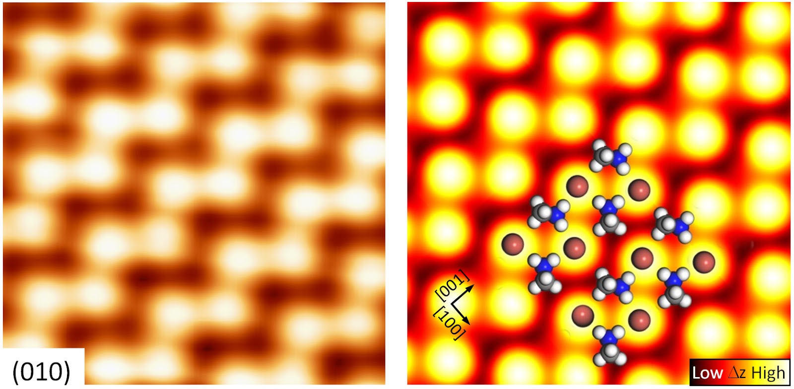
Topography image of atoms of the perovskite crystal and calculated images
with position of atoms and molecules indicated.

(January 8, 2016)  Organic-inorganic perovskite materials are key components of the new generation of solar cells. Understanding properties of these materials is important for improving lifetime and quality of solar cells. Researchers from the Energy Materials and Surface Sciences (EMSS) Unit, led by Prof. Yabing Qi, at the Okinawa Institute of Science and Technology Graduate University (OIST) in collaboration with Prof. Youyong Li’s group from Soochow University (China) and Prof. Nam-Gyu Park’s group from Sungkyunkwan University (Korea) report in the Journal of the American Chemical Society the first atomic resolution study of organic-inorganic perovskite.

Perovskites are a class of materials with the general chemical formula ABX3. A and B are positive ions bound by negative ions X. Organic-inorganic perovskites used in solar cells are usually methylammonium lead halides (CH3NH3PbX3, where X is bromine, iodine, or chlorine). The OIST scientists used a single crystal of methylammonium lead bromide (CH3NH3PbBr3) to create topographic images of its surface with a scanning tunneling microscope.

The researchers discovered that methylammonium molecules (represented by a ball-and-stick model
in the centre) can rotate and that they favour specific orientations that lead to two types of surface
structures with distinctly different properties (left and right images).

This microscope uses a conducting tip that moves across the surface in a manner very similar to a finger moving across a Braille sign. While the bumps in Braille signs are a few millimetres apart, the microscope detects bumps that are more than million times smaller — atoms and molecules. This is achieved by the quantum tunneling effect — the ability of an electron to pass through a barrier. The probability of an electron passing between the material surface and the tip depends on the distance between the two. The resulting atomic-resolution topographic images reveal positions and orientations of atoms and molecules, and also provide a detailed look at structural defects in the surface.
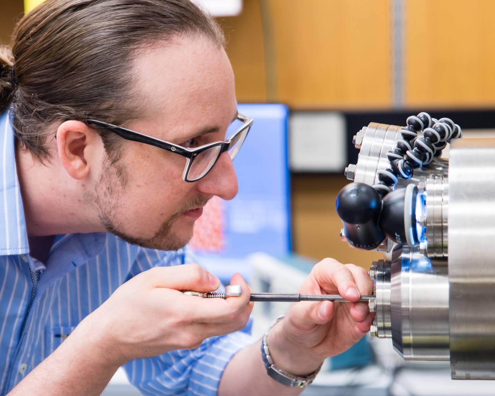
Dr Robin Ohmann, first author of the paper, transfers a sample into the scanning tunneling microscope.

"At room temperature atoms and molecules are quite mobile, so we decided to freeze the crystal to almost absolute zero (-269ºC) to get a good picture of its atomic structure,” says Dr Robin Ohmann, a member of the EMSS Unit and the first author of the paper. The crystal was cut and studied in a vacuum to avoid contamination of the surface. Dr Ohmann's colleagues from Soochow University calculated atomic structures using principles of quantum physics and then compared them with scanning tunneling microscopy data.

read entire press  release >>

Optimum band gap for hybrid silicon/perovskite tandem solar cell


Sketch of the tandem cell. Credit: H. Cords/HZB

(January 8, 2016) Tandem solar cells based on silicon and perovskites have raised high hopes for future high efficiency solar modules.  A team led by perovskite solar cell pioneer Henry Snaith at the University of Oxford has now shown, with contributions by Bernd Rech and Lars Korte of the Helmholtz-Zentrum Berlin, that an ultimate efficiency of 30% should be attainable with such tandem cells. They discovered a structurally stable perovskite composition with its band gap tuned to an optimum value of 1.75 eV. The results have been published in "Science".

Tandem solar cells based on silicon and perovskites have raised high hopes for future high efficiency solar modules (see also results here). A tandem solar cell works by absorbing the high energy photons (visible light) in a top cell which generates a high voltage, and the lower energy photons (Infra red) in a rear cell, which generates a lower voltage. This increases the theoretical maximum efficiency by about 50% in comparison to a standalone silicon cell.

To maximise efficiency, the amount of light absorbed in top cell has to precisely match the light absorbed in the rear cell. However, the band gap of ~1.6eV of the standard perovskite material is too small to fully exploit the efficiency potential of this technology.

A team led by perovskite solar cell pioneer Prof. Henry Snaith FRS at the University of Oxford, in collaboration with silicon solar cell experts Prof. Bernd Rech and Dr. Lars Korte of the Helmholtz-Zentrum Berlin, have shown that an ultimate efficiency of 30% should be attainable with such tandem cells.

They conceived together a tandem cell, in a configuration where the perovskite and  the silicon cell are mechanically stacked and contacted separately. The HZB team contributed the silicon cell. The Oxford group did vary systematically the chemical composition of the perovskite layer, and with a precise cocktail of ions discovered a structurally stable perovsksite  with its band gap tuned to an optimum value of 1.75 electron volts, maintaining a high electronic quality of the layer. At the same time, they increased the chemical and thermal stability of the material significantly.


journal reference >>

Electronically connected graphene nanoribbons foresee high-speed electronics


(January 8, 2016)  Chemical interconnection bridges electronic properties of graphene-nanoribbons with zigzag-edge features.

An international research team at Tohoku University's Advanced Institute of Materials Research (AIMR) succeeded in chemically interconnecting chiral-edge graphene nanoribbons (GNRs) with zigzag-edge features by molecular assembly, and demonstrated electronic connection between GNRs. The GNRs were interconnected exclusively end to end, forming elbow structures, identified as interconnection points (Fig. 1a).

This configuration enabled researchers to demonstrate that the electronic architecture at the interconnection points between two GNRs (Fig. 1b) is the same as that along single GNRs; evidence that GNR electronic properties, such as electron and thermal conductivities, are directly extended through the elbow structures upon chemical GNR interconnection.

This work shows that future development of high-performance, low-power-consumption electronics based on GNRs is possible.

Graphene has long been expected to revolutionize electronics, provided that it can be cut into atomically precise shapes that are connected to desired electrodes. However, while current bottom-up fabrication methods can control graphene's electronic properties, such as high electron mobility, tailored band gaps and s pin-aligned zigzag edges, the connection aspect of graphene structures has never been directly explored. For example, whether electrons traveling across the interconnection points of two GNRs would encounter higher electric resistance remains an open question. As the answers to this type of questions are crucial towards the realization of future high-speed, low-power-consumption electronics, we use molecular assembly to address this issue here.
"Current molecular assemblies either produce straight GNRs (i.e., without identifiable interconnection points), or randomly interconnected GNRs," says Dr. Patrick Han, the project leader. "These growth modes have too many intrinsic unknowns for determining whether electrons travel across graphene interconnection points smoothly. The key is to design a molecular assembly that produces GNRs that are systematically interconnected with clearly distinguishable interconnection points."


journal reference >>

Organic photovoltaics: TUM researchers observe molecular processes


Stephan Pröller (l.) and Dr. Eva M. Herzig in their laboratory. Here they investigate the
processes that take place on the molecular scale during the production of organic solar cells.
(Photo: Uli Benz / TUM)

(January 8, 2016)  X-rays reveal details of plastic solar cell production

Plastic solar cells are light, easy to install, and readily produced using a printer. Nevertheless, the processes that take place on the molecular scale during the production of organic solar cells are not yet entirely clear. Researchers from the Technical University of Munich (TUM) have now managed to observe these processes in real time. Their findings, which are published in the specialist journal Advanced Energy Materials, could help to improve the efficiency of organic solar cells.

The solar modules that can be seen on the roofs of many houses mainly consist of the semiconductor silicon. They are heavy and consequently costly to secure on roofs. Moreover, they do not blend in very well with their surroundings.

Organic solar cells, which consist of organic molecules like plastic bags or cling film, are an alternative to these conventional solar cells. Organic solar cells are soluble and can therefore be produced using a printer. Since they are very thin and light weight the installation of this thin light converting device in a variety of different locations is feasible, furthermore, the color and shape of the solar cells can also be adjusted. One of the current disadvantages is, however: The efficiency of organic photovoltaics has not yet reached that of silicon solar cells.

Processes at the nano level

One of the key parameters for harvesting more energy from the flexible solar cells is the arrangement of the molecular components of the material. This is important for the energy conversion because, as in the case of the "classic" solar cell, free electrons must be produced. To do this, organic solar cells need two types of material, one that donates electrons and another one that accepts them. The interface between these materials must be as large as possible to convert light into electricity. Up to now, it was not known exactly how the molecules align with each other during the printing process and how the crystals they form grow during the drying process. Like the pigments in printer ink, the molecules are initially contained in a solution.


journal reference >>

Mechanical Properties of Nanomaterials Are Altered Due to Electric Field, UW Researchers Find


TeYu Chien, a UW assistant professor in the Department of Physics and Astronomy, uses a
low-temperature scanning tunneling microscope in his lab to observe nanomaterials.
Chien is the lead author of a paper that appears in the journal Scientific Reports. His research
determined that the electric field is responsible for the alteration of the fracture toughness of
nanomaterials, which are used in state-of-the-art electronic devices. (UW Photo)

(January 8, 2016)  Mechanical properties of nanomaterials can be altered due to the application of voltage, University of Wyoming researchers have discovered.

The researchers, led by TeYu Chien, a UW assistant professor in the Department of Physics and Astronomy, determined that the electric field is responsible for altering the fracture toughness of nanomaterials, which are used in state-of-the-art electronic devices. It is the first observed evidence that the electric field changes the fracture toughness at a nanometer scale.

This finding opens the way for further investigation of nanomaterials regarding electric field-mechanical property interactions, which is extremely important for applications and fundamental research.

Chien is the lead author of a paper, titled “Built-in Electric Field Induced Mechanical Property Change at the Lanthanum Nickelate/Nb-doped Strontium Titanate Interfaces,” that was recently published in Scientific Reports. Scientific Reports is an online, open-access journal from the publishers of Nature. The journal publishes scientifically valid primary research from all areas of the natural and clinical sciences.

Other researchers who contributed to the paper are from the University of Arkansas, University of Tennessee and Argonne National Laboratory in Argonne, Ill.

Chien and his research team studied the surfaces of the fractured interfaces of ceramic materials, including lanthanum nickelate and strontium titanate with a small amount of niobium. The researchers revealed that strontium titanate, within a few nanometers of the interfaces, fractured differently from the strontium titanate away from the interfaces.

The two ceramic materials were chosen because one is a metallic oxide while the other is a semiconductor. When the two types of materials come into contact with each other, an intrinsic electric field will automatically be formed in a region, known as the Schottky barrier, near the interface, Chien explains. The Schottky barrier refers to the region where an intrinsic electric field is formed at metal/semiconductor interfaces.


journal reference (Open Access)  >>

Taxi Drones


(January 8, 2016) - Ehang 184

AAV is the safest, Eco-est and Smartest low altitude autonomous aerial vehicle, aiming on providing Medium-Short Distance communication and transportation solution


The 184 AAV is designed with full redundancy – If one set of the power system are operating abnormal, the vehicle can still operate a normal flight plan and ensure the safety of the passenger together with the vehicle.

The 184 was designed to be a 100% with green technology, and is powered by electricity only.

Four arms and eight propellers offer great lifting power and safety. Even with one propeller malfunctions, it can still land in the nearest possible area safely.

The 184 AAV has embedded with Ehangen fail safe system. If any components malfunction or disconnect, the aircraft will immediately land in the nearest possible area to ensure safety.

The communication is encrypted and each AAV has its independent key.

source >>

January 7, 2016

Single-Chip Laser Delivers Powerful Result


 A schematic of the new laser system.

(January 7, 2016)   High power and rapid tuning for the detection of hazardous chemicals

From their use in telecommunication to detecting hazardous chemicals, lasers play a major role in our everyday lives. They keep us connected, keep us safe, and allow us to explore the dark corners of the universe.

Now a Northwestern Engineering team has made this ever-important tool even simpler and more versatile by integrating a mid-infrared tunable laser with an on-chip amplifier. This breakthrough allows adjustable wavelength output, modulators, and amplifiers to be held inside a single package.

With this architecture, the laser has demonstrated an order-of-magnitude more output power than its predecessors, and the tuning range has been enhanced by more than a factor of two.

“We have always been leaders in high-power and high-efficiency lasers,” said Manijeh Razeghi, Walter P. Murphy Professor of Electrical Engineering and Computer Science, who led the study. “Combining an electrically tunable wavelength with high power output was the next logical extension.”


journal reference (Open Access) >>

Partially Oxidized Atomic Cobalt Layers for Carbon Dioxide Electroreduction to Liquid Fuel


(January 7, 2016)  Prof. XIE Yi and Prof. SUN Yongfu’s group from Hefei National Laboratory for Physical Sciences at the Microscale (HFNL)  in the University of Science and Technology of China (USTC) has achieved new progress in the field of atomically-thin two-dimensionalhybrid materials. Their research group constructs a new metal atomic layer with its native oxide, with efforts to disclose the crucial role of surface metal oxide in the electrocatalytic activity of its own metal, adapted from an existing cobalt-based catalyst. This work is published on Jan 4th in Nature with the title of “Partially oxidized atomic cobalt layers for carbon dioxide electroreduction to liquid fuel”.

Electroreduction of CO2 into useful fuels, especially if driven by renewable energy, represents a potentially ‘clean’ strategy for replacing fossil feedstocks and dealing with increasing CO2 emissions and their adverse effects on climate. However, the large barrier of CO2 activation into CO2˙ˉ or other intermediates unfortunately results in impractically high overpotentials, thus enabling it to be the most critical bottleneck in developing efficient CO2 electroreduction. Recently, electrocatalysts based on oxide-derived metal nanostructures were shown to enable CO2 reduction at low potentials. However, it remains unclear how the electrocatalytic activity of these metals is influenced by their native oxides, mainly because microstructural features such as interfaces and defects influence CO2 reduction activity yet are difficult to control.

To tackle all these problems, they construct an ideal model of metal atomic layer with its native oxide to evaluate CO2 reduction in two well-defined catalytic sites. As a prototype, they fabricate 4-atom-thick layers of co-existing Co metal and Co oxide domains, in which the Co oxide domain is embedded in the metallic Co lattice. Base on the electrocatalytic results, they find that surface Co atoms confined in the synthetic 4-atom-thick layers of pure Co metal have higher intrinsic activity and selectivity toward formate production, at lower overpotentials, than surface Co atoms on bulk samples. Compared to the pure Co 4-atom-thick layers, the partially oxidized atomic cobalt layers exhibit further increased intrinsic activity, realizing stable current densities of ~10 mA cm-2 over 40 hours, with ~90% formate selectivity at an overpotential of only 0.24 V, which outperforms previously reported metal or metal oxide electrodes evaluated under comparable conditions. This present work demonstrates that if placed in the correct morphology and oxidation state, a material considered nearly non-catalytic for the CO2 electroreduction reaction can turn into an active catalyst. These findings point to novel opportunities for manipulating and improving the CO2 electroreduction properties of metal systems, especially once the influence of both the atomic-scale structure and the presence of oxide are mechanistically more fully understood.


journal reference >>