
This sequence of
nanolaser images shows a dark-field image of a cesium lead bromide
nanowire (red)
that emits increasingly bright laser light (green) when excited by an
external laser.
(Credit: Sam Eaton/UC Berkeley)
(February 12, 2016) Scientists
at the U.S. Department of Energy’s Lawrence Berkeley National Laboratory
(Berkeley Lab) and UC Berkeley have found a simple new way to produce nanoscale
wires that can serve as tiny, tunable lasers.
The nanowires, with diameters as small as 200 nanometers
(billionths of a meter) and a blend of materials that has also proven effective
in next-generation solar cell designs, were shown to produce very bright,
stable laser light. Researchers say the excellent performance of these tiny
lasers is promising for the field of optoelectronics, which is focused on
combining electronics and light to transmit data, among other applications.
Light can carry far more data, far more rapidly than
standard electronics—a single fiber in a fiber-optic cable, measuring less than
a hair’s width in diameter, can carry tens of thousands of telephone
conversations at once, for example. And miniaturizing lasers to the nanoscale
could further revolutionize computing by bringing light-speed data transmission
to desktop and ultimately handheld computing devices.

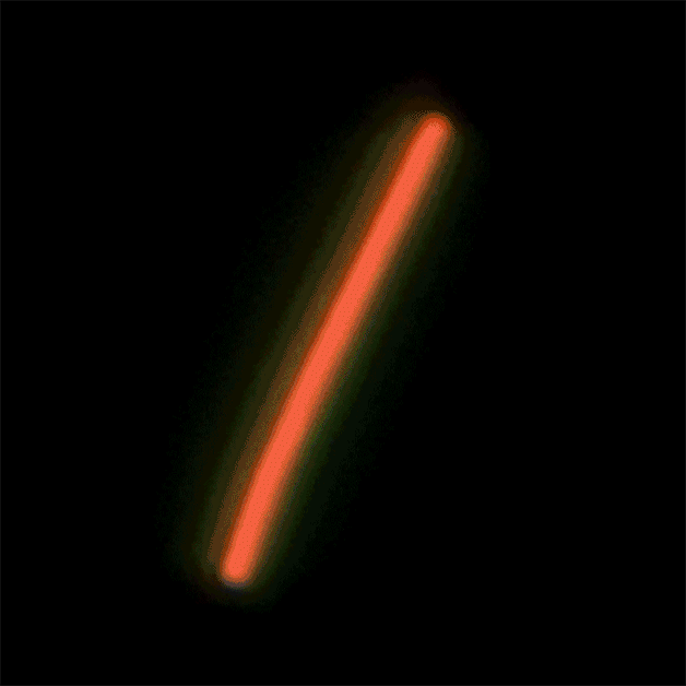
This nanowire,
composed of cesium, lead and bromide (CsPbBr3),
emits bright laser
light after hit by a pulse from another laser source.
The nanowire laser
proved to be very stable, emitting laser light
for over an hour.
It also was demonstrated to be broadly tunable across
green and blue
wavelengths. The white line is a scale bar that measures 2 microns,
or millionths of
an inch. (Credit: Sam Eaton/UC Berkeley)
“What’s amazing is the simplicity of the chemistry here,”
said Peidong Yang, a chemist in Berkeley Lab’s Materials Sciences Division who
led the research, published Feb. 9 in Proceedings of the National Academy of
Sciences. More standard techniques that produce nanowires can require expensive
equipment and exotic conditions, such as high temperatures, and can suffer from
other shortcomings.

A nanowire
construction zone: This scanning electron microscope image shows a collection
of cesium lead
bromide (CsPgbBr3) nanowires and nanoplates grown from a chemical-dipping
process. To
produce these structures, researchers dipped a thin lead-containing film into
a methanol
solution containing cesium, bromine and chlorine heated to about 122 degrees.
The white scale
bar at the lower right represents 10 microns. The image at the bottom left
shows the
well-formed rectangular end of a nanowire—the white scale bar associated with
it
represents 500
nanometers. (Credit: Sam Eaton/UC Berkeley)
The research team developed a simple chemical-dipping
solution process to produce a self-assembled blend of nanoscale crystals,
plates and wires composed of cesium, lead and bromine (with the chemical
formula: CsPbBr3). The same chemical blend, with a molecular architecture
composed of cube-like crystal structures, has also proven effective in an
emerging wave of new designs for high-efficiency solar cells.
“Most of the earlier work with these types of materials is
focused on these solar energy applications,” said Yang, who also holds
appointments with UC Berkeley and the Kavli Energy NanoScience Institute at
Berkeley Lab and UC Berkeley. “There has been so much progress with these
materials in just the past several years—I have a feeling these materials will
open a new research frontier for optoelectronics as well,” he said, and in the
broader field of photonics, which is focused on using light for a range of
applications.