

In MIDI-STEM
(right), developed at Berkeley Lab, an electron beam travels through a ringed
“phase plate,”
producing a high-resolution image (bottom right) that provides details about a
sample containing
a heavy element (gold) and light element (carbon). Details about the carbon
are missing in an
image (bottom left) of the sample using a conventional electron imaging
technique
(ADF-STEM). (Colin
Ophus/Berkeley Lab, Nature Communications: 10.1038/ncomms10719)
(February 29, 2016) Berkeley
Lab-pioneered ‘MIDI-STEM’ produces high-resolution views of lightweight atoms
Electrons can extend our view of microscopic objects well
beyond what’s possible with visible light—all the way to the atomic scale. A
popular method in electron microscopy for looking at tough, resilient materials
in atomic detail is called STEM, or scanning transmission electron microscopy,
but the highly focused beam of electrons used in STEM can also easily destroy
delicate samples.
This is why using electrons to image biological or other
organic compounds, such as chemical mixes that include lithium—a light metal
that is a popular element in next-generation battery research—requires a very
low electron dose.
Scientists at the Department of Energy’s Lawrence Berkeley
National Laboratory (Berkeley Lab) have developed a new imaging technique,
tested on samples of nanoscale gold and carbon, that greatly improves images of
light elements using fewer electrons.
The newly demonstrated technique, dubbed MIDI-STEM, for
matched illumination and detector interferometry STEM, combines STEM with an
optical device called a phase plate that modifies the alternating
peak-to-trough, wave-like properties (called the phase) of the electron beam.
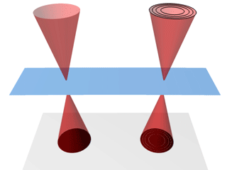
This animated
representation shows a Berkeley Lab-developed technique called
MIDI-STEM (at
right) and conventional STEM (at left) that does not use a ringed object
called a phase
plate. In MIDI-STEM, an interference pattern (bottom right) introduced by
the phase plate
(top right) interacts with the electron beam before it travels through
a sample (the blue
wave in the center). As the phase of the sample
(the distance
between the peaks and valleys of the blue wave) changes,
the electrons
passing through the sample are affected and can be measured
as a pattern
(bottom right). (Colin Ophus/Berkeley Lab)
This phase plate modifies the electron beam in a way that
allows subtle changes in a material to be measured, even revealing materials
that would be invisible in traditional STEM imaging.
Another electron-based method, which researchers use to
determine the detailed structure of delicate, frozen biological samples, is
called cryo-electron microscopy, or cryo-EM. While single-particle cryo-EM is a
powerful tool—it was named as science journal Nature’s 2015 Method of the
Year—it typically requires taking an average over many identical samples to be
effective. Cryo-EM is generally not useful for studying samples with a mixture
of heavy elements (for example, most types of metals) and light elements like
oxygen and carbon.